Yield loss found too late
Defect patterns are identified after lots have already moved on, and root-cause analysis relies on manual correlation across tools.
Industries
Yield engineers must connect flagged inspection images to wafer maps, test logs and process conditions before a lot moves downstream. We build data pipelines and inspection tools that bring that evidence into one review workflow.
Talk about your sector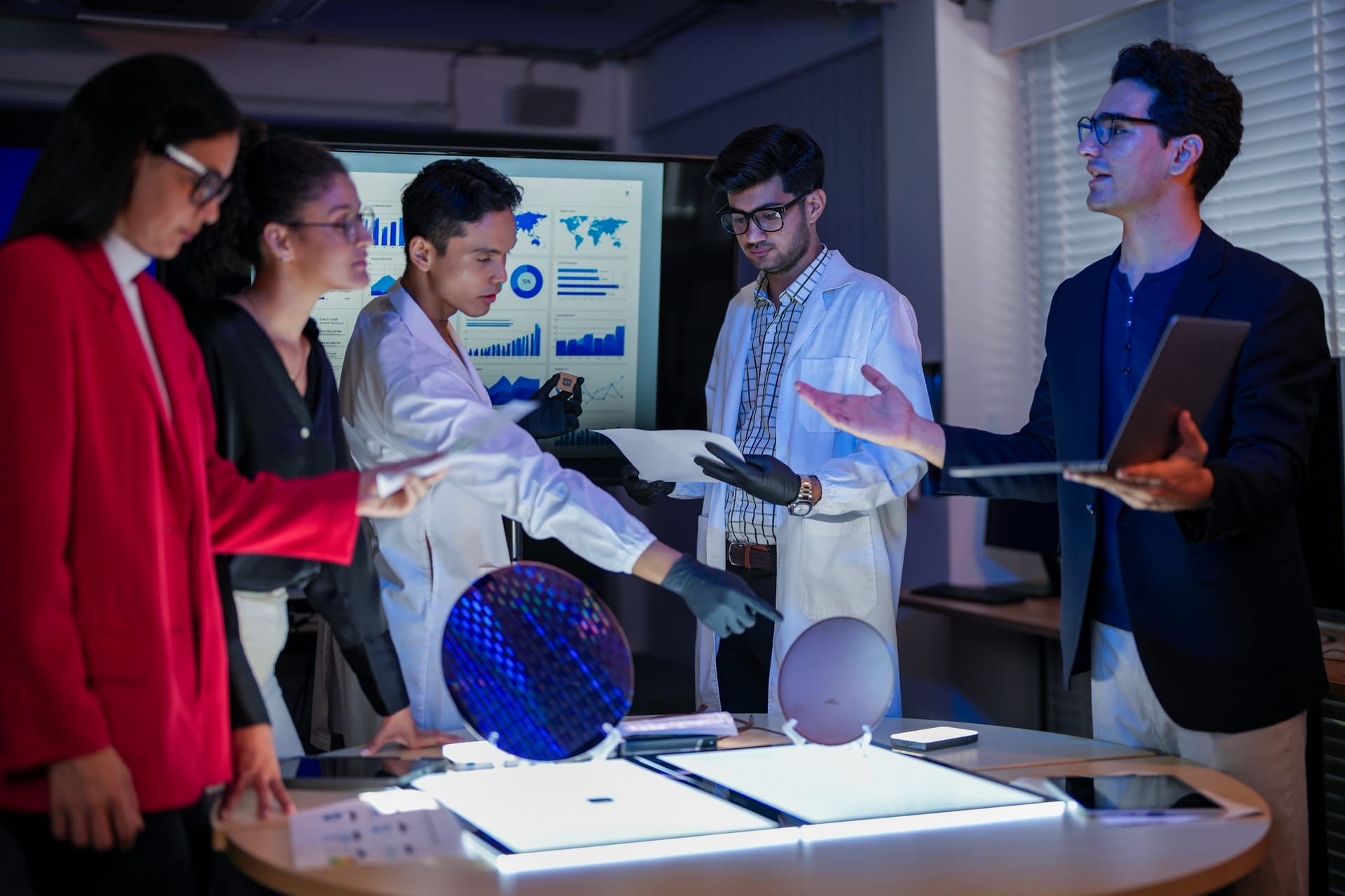
Overview
Semiconductor and hardware companies generate some of the richest engineering data anywhere: wafer maps, test logs, equipment telemetry, inspection images and design files. Most of it is used once and archived. The teams that turn it into yield, throughput and time-to-market gains are the ones that treat data and AI as engineering disciplines, not experiments.
Arixent works with semiconductor manufacturers, fabless companies, equipment makers and hardware product teams on exactly that: analytics platforms for test and yield data, computer vision for inspection, engineering tools that speed up design and validation, and the product engineering behind the software these companies sell alongside their hardware.
Machine Learning, Vision & MLOps: Forecasting, vision and edge models with the MLOps that keeps them reliable after launch.
Data Engineering & Platform Modernization: Batch and streaming pipelines, lakehouses and migrations off legacy warehouses.
Custom Software, SaaS & Mobile: Web platforms, multi-tenant SaaS and mobile apps built to your requirements.
For a representative delivery approach, read Catching wafer defects earlier with computer vision.
Working on this in your sector? Let's compare notes.
Challenges
Defect patterns are identified after lots have already moved on, and root-cause analysis relies on manual correlation across tools.
Terabytes of ATE, parametric and burn-in data sit in silos with no shared model or governed access.
Rule-based optical inspection misses subtle defects and floods engineers with false alarms.
Internal tools for design review, validation and lab management are aging and hard to extend.
Design centers in the US, India and Asia work across systems that do not talk to each other.
Any partner must work inside strict security, data residency and access constraints.
Bring the use case. We will bring the engineering point of view.
Solutions
Governed data platforms and analytics for ATE, parametric and wafer-level data with correlation and root-cause tooling.
Explore this serviceDefect detection and classification on wafer, die and package images with human review for low-confidence cases.
Explore this serviceExcursion prediction, equipment health and process drift models integrated with manufacturing execution systems.
Explore this serviceCustom software for design collaboration, validation tracking, lab management and knowledge search.
Explore this serviceRetrieval-based assistants over specifications, failure analysis reports and process documentation.
Explore this serviceExtended teams and capability centers for software, data and AI work supporting global design and manufacturing sites.
Explore this serviceWhere it fits
FAQ
Related services
Next step
Tell us what you are trying to build and we will come back with a point of view, not a pitch.